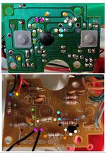
I'm not sure it was necessary to have the entire circuit and path out all the switches and the rest of the resistors and caps.
Could you confirm this:
Here's what I see of the relevant part of the circuit:
Start at what is likely the V+ power rail (it goes to a number of other places).
--to--
A resistor of unknown designation and unknown value (one stripe is red, the rest indistinguishable).
--to--
One side of the speaker (black wire).
Other side of the speaker (other black wire).
--to--
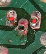
An unused circuit board hole/pad.
--to--
One side of the transistor - presumably collector.
Other side of the transistor - presumably emitter.
--to--
Resistor R6 who's value is 47 *10^something (yellow violet, the rest indistinguishable)
--to--
Ending at what is likely the GND power rail (it goes almost everywhere).
And then the base circuit:
From the COB.
--to--
R7 (220 ohm, i.e. red red brown), C8, and the middle pin of the transistor.
The other side of C8 goes to the presumed GND power rail.
The other side of R7 goes to the anode (i.e. unbanded side) of the small diode.
The diode's cathode (i.e banded side) goes to the presumed GND power rail.
----
I cannot figure out the purpose of the diode! The best answer I can come up with is that the diode biases the transistor's base to 0.7 volts. In other words right at the turn on / turn off point. The COB output might be a digital PWM output. C8 would act as a low pass filter turning the digital signal into a variable voltage.